
Graphene Based Neuromorphic Hardware
Introduction
The most significant structural challenge of the digital age is the physical distance between the processor, where data is handled, and the memory, where it is stored. This bottleneck, known as the "Memory Wall," has become the primary source of the massive energy consumption in modern artificial intelligence systems. However, material science offers a revolutionary solution that brings this static and cumbersome architecture closer to the efficiency of biological systems: Memristors.
The atomic precision of graphene and its derivatives forms the foundation for smart and autonomous devices capable of simultaneously processing and storing information at the point of perception, much like synapses in the human brain. These next-generation photomemristive nanosensors prove that graphene is not merely a passive conductor, but a programmable artificial neural unit that can be rewritten in seconds using light and electricity. By storing data within the material's own physical nature instead of transferring it, this technology reduces energy consumption in the computing world to the atomic level.

Atomic Phase Engineering: Controlling sp² to sp³ Hybridization
The operating principle of graphene-based memristors is built upon more than just electrical conductivity; it relies on the ability to reprogram the material's atomic structure via external stimuli. In its natural state, graphene possesses an sp2 hybridization, where atoms are arranged in a perfect lattice providing superior conductivity. However, the true catalyst behind this technological miracle is graphene's flexible bonding structure: under a controlled electric field or light excitation, the bonds between carbon atoms can locally transform into an sp3 configuration, which exhibits a diamond-like insulating character.
This atomic phase transition dramatically alters the device's electrical resistance, functioning as a memory switch between High Resistance State (HRS) and Low Resistance State (LRS). Due to graphene's single-atom thickness, this transformation occurs at pico-joule levels—meaning data is processed with nearly zero energy consumption. As shown in Figure 1, as the applied external electric field increases, the barrier for atomic bond dissociation drops dramatically, pulling the required energy for phase transition down to the pico-joule scale. The preservation of this atomic alignment even after power is removed allows data to be stored without further energy use. The critical factor here is material perfection; the surface quality and crystalline purity of the graphene and bi-graphene layers are the most fundamental parameters determining the switching speed and the device's operational lifespan over millions of cycles.
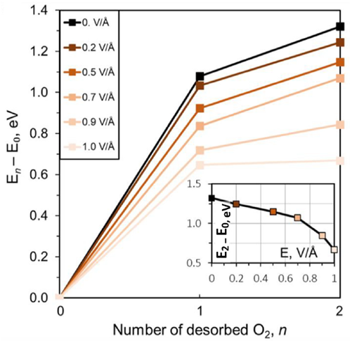
Figure 1. Influence of the external electric field on the energy barrier for atomic bond dissociation (Emelin et al., 2023)
Redox Control and Multiple Conductance States
The technical success of the system relies on the precise management of reduction-oxidation (redox) processes at the interfaces of graphene and graphene oxide (GO). In this architecture, graphene is not merely a passive carrier like a conventional metal electrode; it acts as an ionic gate by hosting the atomic-level movement of oxygen vacancies and ions (VO+ and O-). This ionic migration dynamically modulates graphene’s work function and conductivity, effectively reshaping the device's responsiveness. The characteristic hysteresis loop resulting from this modulation and the stable resistance transitions exhibited over 50 cycles are presented in Figure 2.
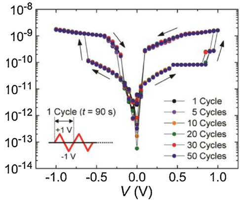
Figure 2. Current-voltage (I-V) characteristics of the memristive heterostructure over 1–50 switching cycles after the application of forming voltage (Emelin et al., 2023).
While traditional silicon-based systems are confined to the rigid boundaries of "0" and "1," the ionic flexibility of graphene electrodes allows for the creation of numerous intermediate conductance states within a single cell. This feature directly emulates synaptic weight changes—the cornerstone of artificial intelligence algorithms—at the hardware level. Consequently, complex datasets are coordinated directly within the graphene interface with ultra-low energy consumption, eliminating the need for an external processor.
Photomemristive Effect: The Light-Driven Artificial Retina
The most striking innovation in this study is the photomemristive heterostructures formed by combining graphene with 2D chalcogenides such as MoS₂ and SnS₂. In this architecture, graphene serves not only as an electrode but also as an optical interface through which charge carriers are transmitted without loss. The asymmetric electrode geometry shown in the Figure 3 (top left) panel allows graphene, thanks to its atomic smoothness, to establish a flawless van der Waals contact with other 2D materials. This atomic compatibility enables the devices to provide an instantaneous response to light across a wide spectral range, extending from ultraviolet to infrared.
While traditional sensors detect light and send data to a remote processor for handling, these graphene-based structures process data at the point of detection by changing their resistance the moment light is perceived. The multi-level photo-response graphs in the Figure 3 (bottom) panel provide hardware-level proof of this in-sensor computing approach; the device classifies different light intensities into distinct conductance steps (HPS1, HPS2, LPS) within its own structure. This feature emulates the function of bipolar cells in the human retina, allowing visual information to be coordinated without the need for an external processor.
These nanosensors, which can be customized according to light wavelength, are capable of retaining data stably over hundreds of cycles even under 0 V bias, as demonstrated in the durability tests in Figure 3 (top right). By eliminating the latency and energy costs associated with data transfer, this technology brings artificial intelligence operations directly down to the hardware level in autonomous vehicles, medical imaging systems, and the defense industry.
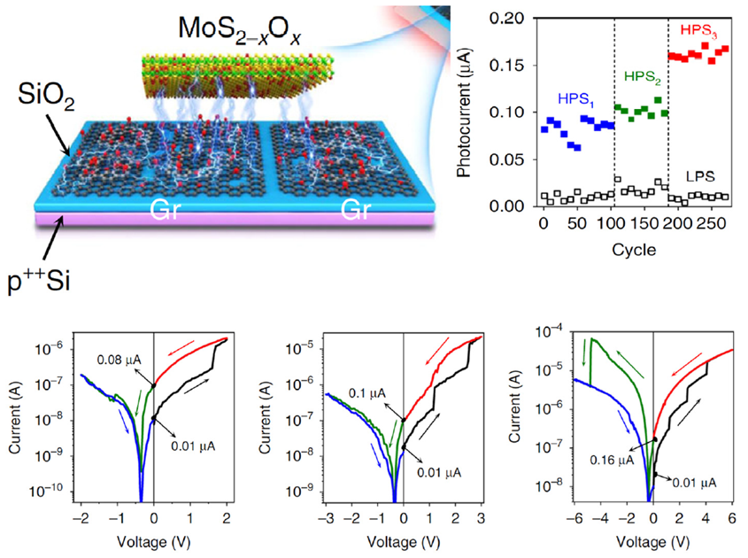
Figure 3. Structural and electrical characterization of the Graphene/MoS₂₋ₓOₓ/Graphene photomemristor: Device schematic (top left), multi-level photo-response switching (bottom), and stable data retention performance under 0 V (top right) (Fu et al., 2023).
Sustainable Nanoenergy and Integration Vision
Graphene-based photomemristors transform the "Nanoenergy" vision from theory to reality with their ability to operate at ultra-low pulse voltages, such as 0.3 V. The greatest advantage of these systems on an industrial scale lies in graphene’s atomic architecture: the absence of dangling bonds on the graphene surface allows for the creation of a flawless interface with existing CMOS infrastructure, even at low temperatures. This "clean integration" capability eliminates the need for the high-cost and complex barrier layers typically required in traditional semiconductor manufacturing.
Scalable through innovative production technologies such as Direct Laser Writing (DLW) or focused electron beams, these structures can be easily integrated into complex circuit schematics, as exemplified by the Ni/GO/Au memristor array presented in Figure 4. When combined with graphene's mechanical flexibility, these photomemristive units offer revolutionary potential, providing high-performance, biocompatible solutions across a wide spectrum—from foldable displays to wearable health sensors and intra-body implants.
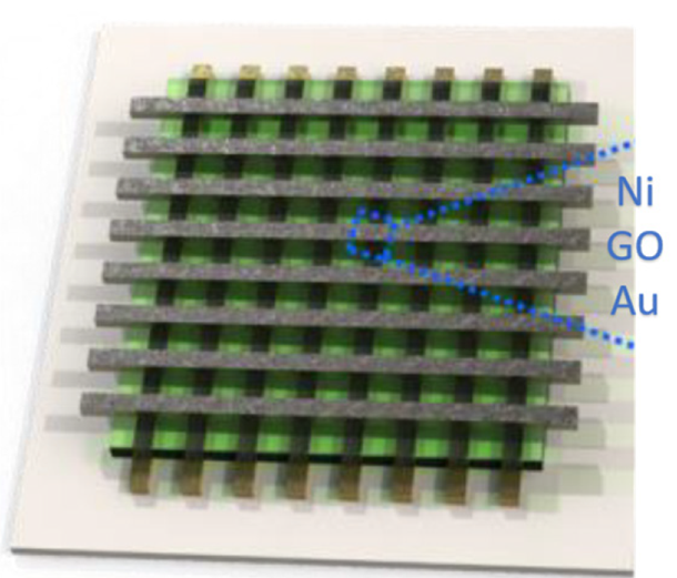
Figure 4. Schematic illustration of the Ni/GO/Au memristor array (Kim et al., 2023).
Conclusion
The evolution of graphene and its derivatives from static components into dynamic ionic transistors and photomemristors—controllable via electricity and light—heralds a new era in material science. Photomemristive mechanisms prove that graphene is not just a conductor, but a decision-making mechanism that brings artificial intelligence down to the hardware level. By pushing efficiency thousands of times beyond that of conventional processors, this technology will dismantle the "memory wall" and serve as the cornerstone for the thinking and remembering autonomous hardware of the future.
At Nanografi, we continue to provide the high-purity graphene, graphene oxide, and 2D nanomaterial solutions that researchers and industrial stakeholders need to bridge the gap from the laboratory to the field. The intelligence of the future is being shaped by the atomic precision of graphene.
References
Emelin, E. V., Cho, H. D., Korepanov, V. I., Varlamova, L. A., Klimchuk, D. O., Erohin, S. V., Larionov, K. V., Kim, D. Y., Sorokin, P. B., & Panin, G. N. (2023). Resistive Switching in Bigraphene/Diamane Nanostructures Formed on a La3Ga5SiO14 Substrate Using Electron Beam Irradiation. Nanomaterials, 13(22), 2978. https://doi.org/10.3390/nano13222978
Fu, X., Li, T., Cai, B., Miao, J., Panin, G. N., Ma, X., Wang, J., Jiang, X., Li, Q., Dong, Y., Hao, C., Sun, J., Xu, H., Zhao, Q., Xia, M., Song, B., Chen, F., Chen, X., Lu, W., & Hu, W. (2023). Graphene/MoS2−xOx/graphene photomemristor with tunable non-volatile responsivities for neuromorphic vision processing. Light: Science & Applications, 12(1). https://doi.org/10.1038/s41377-023-01079-5
Kim, Y., Jeon, S.-B., & Jang, B. C. (2023). Graphene Oxide-Based Memristive Logic-in-Memory Circuit Enabling Normally-Off Computing. Nanomaterials, 13(4), 710. https://doi.org/10.3390/nano13040710
Boroujerdi, R., & Paul, R. (2022). Graphene-Based Electrochemical Sensors for Psychoactive Drugs. Nanomaterials, 12(13), 2250. https://doi.org/10.3390/nano12132250
Panin, G. N. (2026). Graphene-Based Memristive and Photomemristive Nanosensors for Energy-Efficient Information Processing. Nanoenergy Advances, 6(1), 6. https://doi.org/10.3390/nanoenergyadv6010006
Recent Posts
-

Anode Materials for Sodium-Ion Batteries: A Technical Guide
Sodium-ion batteries are gaining serious commercial momentum. First-generation cells are already rea …15th Jun 2026 -

Nanoclay: Properties, Production, Applications
Nanoclay is a component composed of phyllosilicates, which are compounds based on the elements of ox …12th Jun 2026 -

Cathode Materials for Sodium-Ion Batteries: A Technical Guide
Lithium-ion batteries have dominated the energy storage landscape for decades. Yet rising demand for …3rd Jun 2026