
Printed Electronics: Materials and Applications
Electronics no longer have to be rigid, bulky, or expensive to manufacture. Printed electronics — the process of depositing functional materials onto substrates using printing techniques — is changing how circuits, sensors, and antennas are made. Instead of etching copper away from a board, you print what you need, where you need it, on surfaces as thin and flexible as a sheet of paper. The global market reflects the momentum: valued at roughly USD 19 billion in 2025, it is forecast to grow at a double-digit rate through the next decade, driven by demand for wearable devices, smart packaging, and IoT sensors (Grand View Research, 2025).
At the heart of printed electronics is a deceptively simple question: what material goes in the ink? The answer determines everything: the electrical conductivity and charge transport behavior, the electromechanical stability under strain, and the thermal budget of the substrate during processing.
This article walks through the three main material families used in printed electronics today, explains what makes each one suited to different applications, and points to where the field is heading.
What Is Printed Electronics? A Material-Centric Definition
Printed electronics is an additive manufacturing approach in which functional electronic materials and patterns are deposited onto a substrate using scalable printing techniques rather than subtractive photolithographic processes. Unlike conventional PCB fabrication, which removes material through etching and generates significant chemical waste, printed electronics deposit only what is needed, where it is needed, with high material utilization efficiency.
The defining characteristic of printed electronics is not the printing method itself — whether screen printing, inkjet, aerosol jet, gravure, or flexographic — but the functional material being deposited. The ink or paste must carry the right combination of particle size, viscosity, surface tension, electrical conductivity, and post-processing mechanisms (curing, sintering, or drying) to produce a reliable electronic function on the final substrate.
This is why printed electronics is fundamentally a materials science problem before it is a manufacturing problem. Choosing the right conductive, semiconductive, or resistive material determines whether a printed circuit will operate reliably over thousands of flex cycles on a polyimide film or deliver consistent electrochemical response on a paper-based biosensor.
The Core Material Categories in Printed Electronics
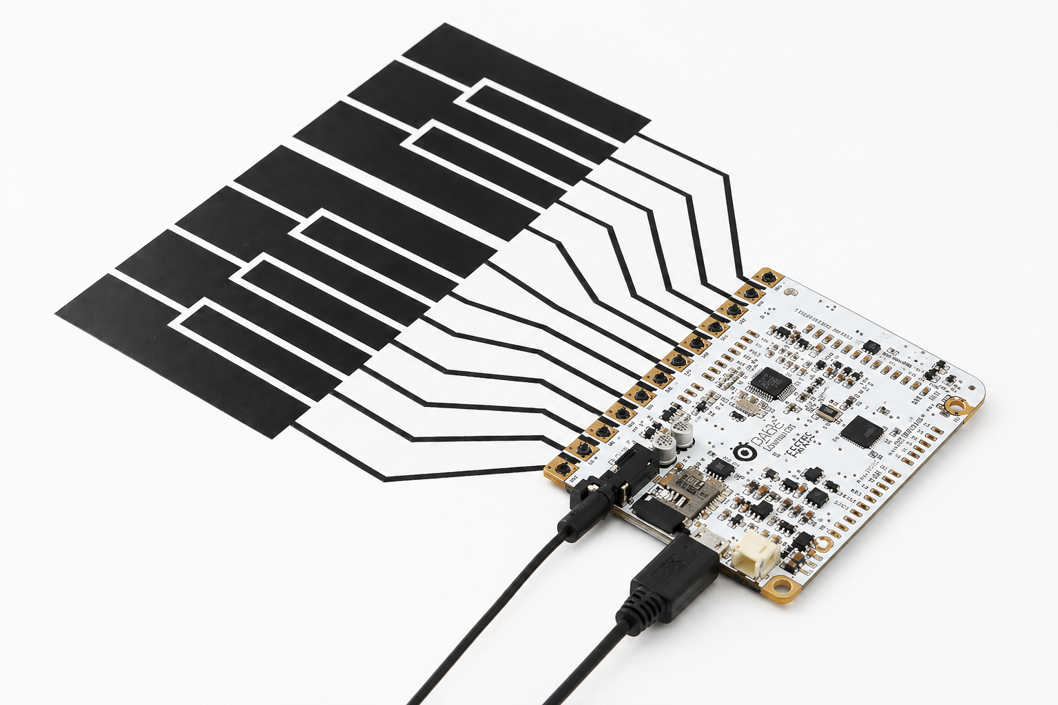
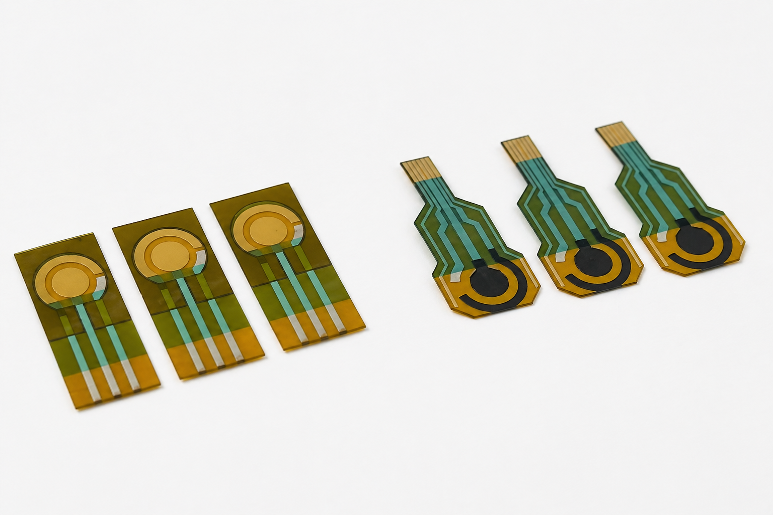
Silver: The Default Choice for High Conductivity
Silver is the most electrically conductive metal, and its nanoparticle form is the backbone of the conductive ink market, accounting for around 78% of total printed electronics material revenue in 2025. Unlike copper, silver oxides are either unstable or intrinsically conductive which means silver-based traces remain reliable even when exposed to air during processing.
The reason silver nanoparticle inks work on flexible plastic substrates is a nanoscale effect: nanoparticles undergo coalescence and sintering at temperatures far below bulk silver's melting point. Processing advances in recent years have pushed this further — silver tracks can now be sintered at temperatures as low as 85 °C using moisture-assisted methods, making it possible to print on heat-sensitive substrates that previously could not be used.
Silver paste is standard for screen-printed RFID antennas, solar cell contacts, membrane switches, and flexible heaters. For inkjet and spray coating, where lower viscosity is essential, silver nanoparticle inks offer the same material in liquid form, compatible with fine-feature printing.
Nanografi offers silver formulations across this range: Silver Paste for screen printing, Silver Conductive Adhesive Paste for microelectronic packaging, and Silver Dispersions for inkjet and spray deposition.
Carbon: Stability, Versatility, and Cost
Carbon does not match silver's conductivity, but it brings advantages silver cannot: electrochemical stability, low cost, and a variety of allotropes including graphite, carbon black, graphene, carbon nanotubes. Each suited to a different role.
Carbon paste (graphite or carbon black in a polymer binder) is the workhorse for biosensor electrodes, resistive heating elements, and humidity sensors. It is chemically inert in electrochemical environments where silver would corrode or interfere with measurements, and it screen-prints reliably onto flexible substrates. Nanografi's Carbon Paste is formulated for single-pass printing with stable electrical output.
Carbon nanotube (CNT) paste is a step up in performance. CNTs are effective at very low concentrations because each nanotube has a high aspect ratio — a sparse network of tubes can form percolation networks through a film without needing high filler loading. The result is thinner printed layers, better mechanical flexibility, and less material per unit area. Nanografi's water-based Carbon Nanotube Paste achieves competitive sheet resistance without organic solvents, which simplifies handling and broadens substrate compatibility.
More on carbon nanotubes: Single-Walled Carbon Nanotubes and Double-Walled Carbon Nanotubes on Nanografi Blografi.
Graphene: The High-Potential Material
Graphene is a single layer of carbon atoms arranged in a hexagonal lattice. Its theoretical properties İnclude high carrier mobility, mechanical strength, optical transparency, and flexibility. These properties are exceptional across almost every dimension relevant to printed electronics. The practical reality is more nuanced, but improving steadily.
Printed graphene is typically few-layer graphene produced by liquid-phase exfoliation in a liquid medium, or one of its derivatives: graphene oxide (GO) or reduced graphene oxide (rGO). GO disperses easily in water, making it straightforward to formulate into water-based inks, but requires chemical or thermal reduction to become conductive. rGO recovers a significant portion of graphene's conductivity after reduction and is increasingly used as a lower-cost, more processable alternative in sensors, coatings, and energy storage electrodes.
Recent research has demonstrated screen-printed graphene conductors maintaining stable electrical performance through repeated bending cycles, with hybrid graphene–CNT inks achieving sheet resistance parity with carbon paste without any sintering step. These results are making graphene-based inks increasingly viable for transparent electrodes, flexible displays, and wearable electrochemical sensors.
Nanografi's Graphene Dispersions cover pristine graphene, GO, and rGO in water, ethanol, and NMP. Graphene Nanoplatelets are available for higher-solid-loading paste formulation.
Further reading: Graphene Nanoplatelets: Electrical Properties & Applications and Applications of Reduced Graphene Oxide.
How Do Substrate and Printing Method Affect Material Choice?
Every material decision in printed electronics is shaped by two constraints: what the substrate can tolerate and what the printing method requires.
PET (the most widely used flexible substrate) is limited by its low glass transition temperature, which rules out high-temperature sintering and points toward low-temperature sintering silver pastes or water-based CNT formulations. Polyimide handles much higher temperatures and opens the door to solderable silver pastes. Paper supports ultra-low-cost single-use diagnostics using water-compatible graphene or CNT inks. Textiles need thixotropic pastes that can anchor to rough, porous surfaces.
The printing method adds another layer. Screen printing suits thick, high-viscosity pastes and high-volume production — it currently holds the largest share of the printed electronics technology market. Inkjet printing is the fastest-growing method, valued for its precision and minimal material waste, but it requires inks with much lower viscosity, which limits the particle mass fraction and therefore the achievable conductivity per pass. Most real-world printed electronics processes are built around finding the right compromise between these parameters.
Where Is Printed Electronics Heading?
The applications driving growth share a common thread: they need electronics to be lightweight, flexible, and manufacturable at scale bypassing high-vacuum and cleanroom-intensive semiconductor fabrication. Wearable biosensors for continuous health monitoring, printed NFC and RFID antennas, flexible photovoltaic films, and smart packaging that integrates with supply chain systems are all moving from research into production.
The materials enabling this shift — silver, carbon, graphene — are commercially available today. What is advancing rapidly is the understanding of ink rheology, deposition kinetics, and high-throughput processing reliably on non-conventional substrates, at speeds and costs that make large-area, roll-to-roll compatible electronics viable at scale. That is where the most consequential materials science in this field is happening right now.
Frequently Asked Questions
What is the difference between conductive paste and conductive ink in printed electronics? The terms are often used interchangeably, but they refer to distinct rheological profiles and viscosity ranges. Pastes are thick, high-solid-loading formulations designed for screen printing, where the squeegee forces material through a mesh. Inks are low-viscosity formulations designed for inkjet, aerosol jet, or gravure printing, where the material must flow through fine nozzles or be transferred from a smooth roller. The same functional material (silver, carbon, graphene) can be formulated as either, depending on the printing method it is intended for.
Why are carbon nanotubes used in printed electronics despite being more expensive than graphite? CNTs form conductive networks at very low concentrations because of their geometry. Each tube is thousands of times longer than its diameter. This means you need far less material to reach the percolation threshold compared to graphite paste, and the resulting printed film is thinner and more mechanically flexible. For applications like wearable sensors or conformable electronics, those properties justify the higher material cost.
Can printed electronics match the performance of conventional PCBs? For most high-frequency, high-power applications, no — conventional PCBs still have an advantage in dimensional precision, bulk conductivity and dielectric performance. But printed electronics is not intended to replace rigid PCBs; it targets applications where flexibility, large-area coverage, low cost, or substrate diversity are the priority. Printed RFID antennas, biosensors, and flexible displays are examples where printed approaches are already the preferred manufacturing route.
What substrates are compatible with printed electronics? The most common are PET film, polyimide (Kapton), paper, and textiles. Each has a different thermal degradation profiles and glass transition temperatures, surface energy, and mechanical behaviour that constrains which inks and curing conditions can be used. PET is the most widely used due to its low cost and broad ink compatibility. Polyimide is preferred when high processing temperatures are needed. Paper enables disposable, low-cost diagnostic devices. Textiles require specially formulated pastes that bond to irregular, porous surfaces.
Is graphene replacing silver in conductive inks? Not at the moment, and likely not across the board. Graphene-based inks offer advantages in transparency, electrochemical stability, and flexibility, but they do not yet match sintered silver paste İn terms of ultra-low sheet resistance for RF applications. The more accurate picture is that graphene is expanding the range of what printed electronics can do — enabling applications like transparent conductive electrodes and wearable biosensors where silver would be unsuitable — rather than Complementing the material palette in existing applications.
Further Resources on Functional Inks
Printed electronics applications are ultimately defined by how materials are formulated into functional inks and pastes. From conductive silver systems to carbon-based and graphene-enabled formulations, the transition from material to application depends on precise ink engineering and process compatibility. For a deeper look into formulation strategies, application-specific ink systems, and scalable printing solutions, you can explore Nanografi’s dedicated platform for functional and security inks at https://inks.nanografi.com/.

Nanografi Products Referenced in This Article
- Conductive Adhesive Pastes
- Silver Dispersions
- Graphene Dispersions
- Graphene Nanoplatelets
- Single-Walled Carbon Nanotubes
- Multi-Walled Carbon Nanotubes
Related reading: What is Conductive Carbon Paste? · Explained: Silver Nanoparticles · Silver Nanowires & Applications · Graphene Nanoplatelets: Electrical Properties & Applications
References
- Grand View Research. (2025). Printed Electronics Market Size, Share & Trends Analysis Report, 2026–2033. https://www.grandviewresearch.com/industry-analysis/printed-electronics-market
- MarketsandMarkets. (2025). Printed Electronics Market – Global Forecast to 2030. https://www.marketsandmarkets.com/Market-Reports/printed-electronics-market-197.html
- SNS Insider. (2026, April 21). 3D Printed Electronics Market Size to Worth USD 74.58 Billion by 2035. Globe Newswire. https://www.globenewswire.com/news-release/2026/04/21/3278166
- Chen, Z., Gengenbach, U., Koker, L., et al. (2024). Systematic investigation of novel, controlled low-temperature sintering processes for inkjet printed silver nanoparticle ink. Small, 20(21), e2306865. https://doi.org/10.1002/smll.202306865
- Mo, L., Guo, Z., Yang, L., et al. (2019). Silver nanoparticles based ink with moderate sintering in flexible and printed electronics. International Journal of Molecular Sciences, 20(9), 2124. https://doi.org/10.3390/ijms20092124
- Campos-Arias, L., Arrese-Igor, S., Obande, W., et al. (2024). Stretchable conductive inks with carbon-based fillers for conformable printed electronics. Advanced Engineering Materials, 26(18), 2400354. https://doi.org/10.1002/adem.202400354
- Xin, Z., Yan, Z., Tan, C., et al. (2022). Large-scale production of electrothermal films with GNSs/CNTs/CB three-dimensional structure ink by screen printing. ACS Applied Electronic Materials, 4(2), 536–546. https://doi.org/10.1021/acsaelm.1c01172
- Karunakaran, S. K., Arumugam, G. M., Yang, W., et al. (2021). Highly concentrated, conductive, defect-free graphene ink for screen-printed sensor application. npj Flexible Electronics, 5(1), 1. https://doi.org/10.1038/s41528-021-00097-0
- ScienceDirect. (2025). Inkjet printing of conductive nanomaterials on textiles for wearable electronics. Progress in Organic Coatings, 199, 109038. https://doi.org/10.1016/j.porgcoat.2025.109038
Recent Posts
-

Anode Materials for Sodium-Ion Batteries: A Technical Guide
Sodium-ion batteries are gaining serious commercial momentum. First-generation cells are already rea …15th Jun 2026 -

Nanoclay: Properties, Production, Applications
Nanoclay is a component composed of phyllosilicates, which are compounds based on the elements of ox …12th Jun 2026 -

Cathode Materials for Sodium-Ion Batteries: A Technical Guide
Lithium-ion batteries have dominated the energy storage landscape for decades. Yet rising demand for …3rd Jun 2026