
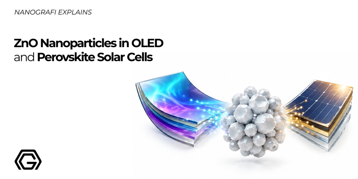
ZnO Nanoparticles in OLED and Perovskite Solar Cells
Many printed solar cells and inverted display stacks need a layer that collects electrons and passes them to the electrode. For a long time that layer meant titanium dioxide and a furnace running at several hundred degrees. Zinc oxide nanoparticles changed that. They form a dense, transparent, conductive film straight from an alcohol dispersion at room temperature, which is why ZnO is now a widely used electron transport material in perovskite solar cells, OLEDs, QLEDs and perovskite LEDs.
ZnO also comes with one well known complication, and knowing how to design around it is the difference between a device that lasts and one whose active layer degrades during thermal processing. This guide covers both sides: what ZnO does well, where it fails, and how to pick the right grade for the job.
Why ZnO Nanoparticles Replaced High Temperature Metal Oxides
Conventional mesoporous titania scaffolds can require sintering at temperatures of up to 500 °C. That rules out plastic substrates, adds a slow step to the line, and makes roll to roll manufacturing impractical. A colloidal ZnO nanoparticle layer can be processed without high-temperature sintering. After spin coating and solvent evaporation, a functional film can be obtained.
The performance did not have to be sacrificed for that convenience. Room temperature processed ZnO layers carried planar perovskite cells to 15.7% power conversion efficiency in the work that established the approach, and the same route produced flexible cells above 10% on plastic. Once that was demonstrated, the electron transport layer stopped being a ceramics problem and became a coating problem.
Three properties do the work here. ZnO is a wide bandgap semiconductor, so it stays transparent across the visible range and can sit on the illuminated face of a cell or the viewing face of a display. It is natively n-type, so it conducts electrons without doping. ZnO can also be synthesised as well-faceted nanocrystals and formulated as stable, coatable alcohol-based dispersions when its particle size and surface chemistry are appropriately controlled. Our guide to the fundamental properties and applications of zinc oxide nanoparticles covers the crystallography in more depth.
How ZnO Moves Electrons in a Device Stack
The conduction band of ZnO can be favourably aligned with those of lead halide perovskites and CdSe- or InP-based core-shell quantum dots. This alignment can facilitate electron transfer across the interface.
In a solar cell this is exactly what you want. Electrons generated in the absorber need to be extracted efficiently, and favourable energy-level alignment can reduce interfacial losses and support a high output voltage.
In a light-emitting device, the same property can contribute to charge imbalance. Electrons arrive at the emissive layer faster than holes arrive from the other side. The surplus electrons do not all turn into light. Some may leak through the emissive layer or accumulate at interfaces and accelerate degradation, while direct contact with ZnO and defect-assisted interfacial charge transfer can quench excitons. A major objective in ZnO-based QLED and OLED design is therefore to balance electron and hole injection while suppressing interfacial exciton quenching.
This is the single most useful thing to understand before choosing a grade. Solar cell work optimises ZnO for extraction speed and chemical stability. Display work optimises it for a raised conduction band, a higher work function and separation from the emitter. The starting powder can be identical. What you do to its surface is not.
ZnO Electron Transport Layers in Perovskite Solar Cells
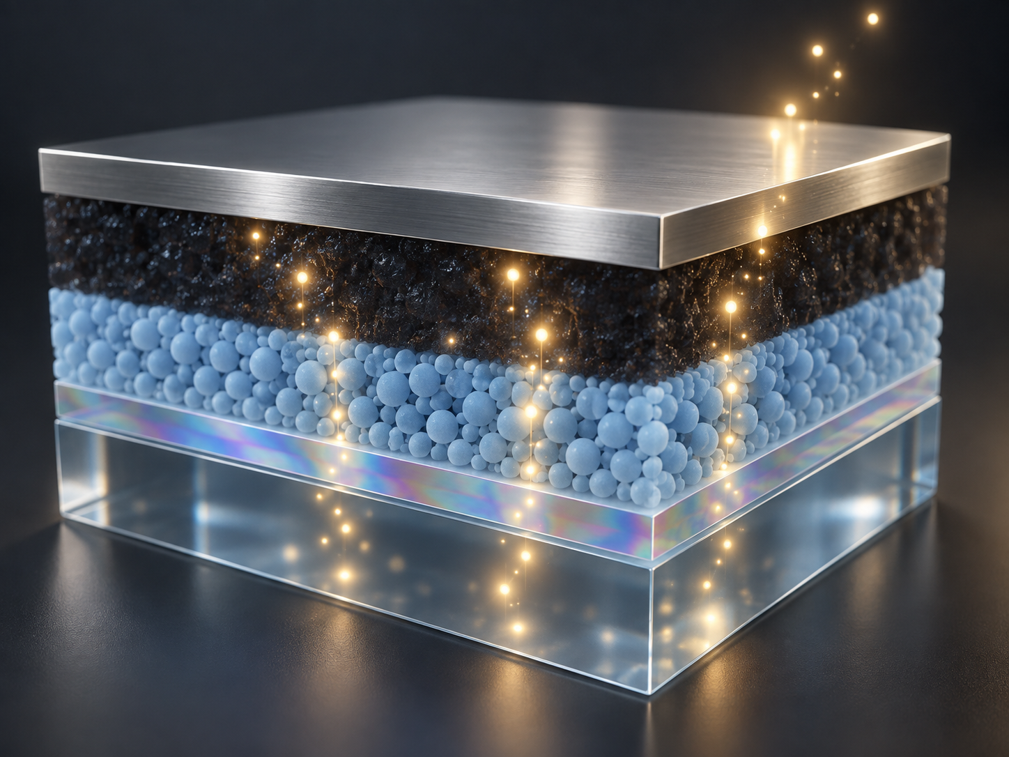
In a conventional planar n–i–p cell, the ZnO film sits between the transparent electrode and the absorber, usually a few tens of nanometres thick, deposited by spin coating or slot die coating from an alcohol dispersion.
Compared with conventionally processed compact titanium dioxide, ZnO can eliminate the need for high-temperature annealing. Compared with tin dioxide, ZnO generally has a more chemically reactive surface, while their relative electron mobility depends strongly on material quality and processing conditions. Those are the real trade offs, and which one wins depends on your absorber composition and your thermal budget. If your process cannot tolerate a reactive oxide at the absorber interface, tin dioxide nanoparticles are the usual substitution, and titanium dioxide nanoparticles remain an option where the furnace step is acceptable. On the hole side of an inverted stack, nickel oxide nanoparticles are a widely used solution-processed counterpart.
Doping is an established way to tune the electronic and interfacial properties of the layer. Lithium passivates defects in the ZnO lattice and lowers the barrier electrons have to cross. Aluminium doping can increase electrical conductivity while maintaining high optical transparency, and it can also reduce the interfacial reactivity of ZnO. Magnesium raises the conduction band. All three can be compatible with deposition methods used for undoped ZnO, although their formulation and processing conditions may require optimisation. For background on why this absorber class attracts the effort, see our overview of perovskites in energy conversion technologies.
The Problem You Have to Design Around: Perovskite Decomposition on ZnO
A major failure mechanism in ZnO-based perovskite devices is chemical rather than electrical, and it is worth stating plainly.
The surface of a ZnO nanoparticle can contain hydroxyl groups and, depending on the synthesis route, residual acetate species. That surface is basic. When a methylammonium lead iodide film is deposited on top and annealed, the surface pulls a proton off the methylammonium cation. The cation becomes methylamine, which evaporates. The perovskite loses its A site cation and what remains is lead iodide. You see it as the film turning yellow on the hotplate.
There are four established ways to deal with it, and they combine well:
- Dope the lattice. Doping or alloying ZnO with elements such as aluminium, lithium, magnesium or silver can modify its defect chemistry and interfacial reactivity, although the effects depend on the dopant and its concentration. Aluminium doped ZnO in particular is known for giving thermally stable perovskite films.
- Passivate during synthesis. Treating the nanoparticles with an amine such as ethanolamine caps the reactive sites before the perovskite ever touches them, and cells built this way have exceeded 18% efficiency.
- Insert a buffer. A thin interlayer between the ZnO and the absorber keeps the two chemistries apart. PCBM is one of the established choices and evaporated tungsten oxide has been used to the same effect.
- Use a shell. Growing a thin zinc sulfide shell on the ZnO core can reduce surface hydroxyl species and passivate oxygen-vacancy-related defects, suppressing both the deprotonation reaction and trap assisted recombination, while keeping electron mobility close to that of bare ZnO.
There is also a fifth route that sits in the absorber rather than the oxide. Methylammonium-free formulations avoid the specific methylammonium deprotonation pathway, and formamidinium–caesium compositions generally show improved interfacial stability on ZnO.
The practical consequence for purchasing is simple. Surface hydroxyl and residual acetate content of the powder is a functional specification, not a cosmetic one. Ask about the synthesis route.
ZnO Electron Injection Layers in OLED and QLED Displays
A conventional OLED often uses a low-work-function metal or a metal combined with an electron-injection layer as the cathode, and air-sensitive cathode structures require encapsulation. In an inverted architecture, a transparent conductive oxide serves as the bottom cathode-side electrode, while an adjacent electron-injection layer facilitates electron transfer into the organic layers. ZnO nanoparticles can bridge the energy-level and interfacial gap between that oxide and the organic layers above it, and inverted phosphorescent OLEDs have been built on a single ZnO nanoparticle injection layer without the usual stack of interlayers.
In QLEDs, the ZnO layer performs a similar function adjacent to the quantum-dot emissive layer. Two important loss mechanisms are electron–hole imbalance and interfacial exciton quenching, the latter of which can occur where the quantum dots directly contact ZnO. They need different fixes. Appropriately increasing the work function of ZnO can reduce excessive electron injection and improve charge balance. Introducing an ultrathin insulating or molecular interlayer between the quantum dots and ZnO can suppress interfacial exciton quenching. Doing both at once, with a molecular interlayer that raises the work function and separates the two materials, has more than doubled current efficiency in inverted QLEDs.
Operating lifetime is strongly influenced by defect chemistry as well as charge balance and interfacial stability. Oxygen-vacancy-related defect states in the ZnO film can act as electron traps, and passivating them with fluorine has extended red QLED lifetime by more than an order of magnitude. This makes oxygen vacancy density a genuine procurement question rather than an academic one.
Our QLED quantum dots are specified for use with a ZnMgO nanoparticle solution as the electron transport layer to support controlled electron injection and improved charge balance. The wider quantum dot range covers CdSe/ZnS, InP/ZnS, ZnSe/ZnS, PbS, carbon and graphene chemistries.

ZnMgO, Bilayers and Doped ZnO: Tuning the Electron Supply
Alloying zinc oxide with magnesium widens its bandgap and shifts its conduction-band position, while also modifying its work function. ZnMgO can be deposited using methods similar to those used for ZnO, although the formulation and processing conditions may require adjustment. ZnMgO is a widely used option for controlling electron injection when undoped ZnO causes excessive electron supply to the emissive layer, and it is used either as the full transport layer or as a thin interlayer between a ZnO film and the quantum dot layer.
Stacking is the other approach. In the reported SnO₂/ZnO bilayer architecture, placing a solution-processed SnO₂ layer underneath ZnO and keeping ZnO next to the emitter lets the lower layer meter the electron supply while the ZnO smooths the surface and keeps injection efficient. A related bilayer approach has also been reported in photovoltaics, where ZnO/SnO₂-based electron-transport structures can improve the open-circuit voltage of planar cells.
Where solution processing cannot provide the required film uniformity or thickness control, atomic layer deposition or sputtering can be considered; atomic layer deposition is particularly suitable when conformal coverage is required. For sputtering processes we supply zinc oxide sputtering targets and aluminium doped zinc oxide targets.
Powder or Dispersion: Choosing the Right ZnO Form
A ZnO layer is only as good as the liquid it was cast from. Agglomerates comparable to or larger than the film thickness can create surface defects, pinholes and shunt pathways. A dispersion that settles in storage gives you a different thickness every week. This is the part of the process most teams underestimate.
Solvent first. Alcohols such as ethanol and isopropanol can provide solvent orthogonality with many device layers, although their compatibility with the specific organic transport material or perovskite composition must be verified. They can wet appropriately prepared transparent electrodes and evaporate at relatively low temperatures, although a drying or low-temperature annealing step may still be required. That makes a ZnO dispersion in ethanol at 20 wt% a useful stock dispersion for device development, provided that its concentration and coating conditions are adjusted for the required film thickness. A water based ZnO dispersion at the same loading suits coatings, composites and photocatalytic formulations, where water compatibility matters more than solvent orthogonality.
Surface chemistry second. A silane treated grade such as our 18 nm ZnO with KH550 aminosilane disperses easily in organic media and resists reagglomeration, which is what you want in a polymer composite or a solvent borne coating. For a charge-transport layer, an organic surface treatment may impede interparticle electron transport and increase series resistance if it forms an excessively insulating barrier. Device applications therefore require low-residue ZnO or a deliberately selected surface treatment whose effect on charge transport has been verified.
| What to check | Why it matters |
| Primary particle size | Should generally be smaller than the target film thickness; larger particles or agglomerates can increase surface roughness and cause film defects or pinholes |
| Agglomerate size in the dispersion | Influences shunt-path formation, film uniformity and thickness repeatability. Ask for data on the liquid as supplied, not on the dry powder |
| Purity and elemental profile | Some transition-metal residues can act as recombination centres and degrade device performance |
| Specific surface area | A useful indicator of accessible surface area and effective particle size; surface hydroxyl content requires separate surface-chemical analysis |
| Synthesis route and post treatment | Influences the amount of surface hydroxyl and residual acetate species, which can contribute to perovskite decomposition |
| Surface treatment | Silane treatment can improve dispersion but may increase electrical resistance. Low-residue or appropriately surface-modified grades should be evaluated for device layers, while silane-treated grades are generally better suited to composites |
ZnO Nanoparticle Grades from Nanografi
All grades share CAS number 1314-13-2 and ship from our zinc oxide nanoparticle range, part of a wider nanoparticle catalog.
- ZnO nanopowder, 99.5% purity, 20 to 30 nm, specific surface area 30 to 50 m²/g. The general purpose grade for formulating your own electron transport ink.
- ZnO nanopowder, 99.5+% purity, 30 to 50 nm, for thicker functional layers and composite loading.
- ZnO nanopowder, 99.5+% purity, 18 nm, KH550 treated, nearly spherical single crystal particles with 1 wt% aminosilane. The dispersion optimised grade.
- ZnO dispersion in ethanol, 20 to 30 nm, 20 wt%, ready to dilute for spin coating and slot die coating.
- ZnO water dispersion, 20 to 30 nm, 20 wt%, for aqueous coatings, composites and photocatalytic systems.
- Zinc oxide micron powder, where nanoscale size is not needed, as in ceramics, rubber and varistors.
Need a doped grade, a different solvent or a different solid loading? Contact us and we will quote against your specification.
Frequently Asked Questions
Why use ZnO instead of TiO₂ in a perovskite solar cell?
Because ZnO nanoparticle layers can be processed without high-temperature sintering. Conventionally processed mesoporous titania can require temperatures of up to 500 °C, whereas ZnO nanoparticle layers can be deposited and processed at substantially lower temperatures. That opens the door to plastic substrates and roll to roll production, and the approach still reached 15.7% efficiency in planar cells.
Why do perovskite films turn yellow on ZnO?
The basic, hydroxylated ZnO surface strips a proton from the methylammonium cation. The cation leaves as methylamine and the perovskite converts to lead iodide. Doping, surface passivation, a buffer layer or a ZnS shell can reduce this degradation, while methylammonium-free absorbers avoid the specific methylammonium-deprotonation pathway.
What is ZnMgO and when should I use it instead of ZnO?
ZnMgO is zinc oxide alloyed with magnesium, which widens the bandgap and shifts the conduction-band position while modifying the work function. It can be used in QLEDs and inverted OLEDs when the electron injection provided by ZnO must be adjusted to improve electron–hole balance. In solar cells, undoped or appropriately doped ZnO may be selected according to the required band alignment, defect density and interfacial stability.
Should I buy ZnO powder or a ready made dispersion?
Take the dispersion if you are coating device layers and need repeatable film thickness, because redispersing dry nanopowder to a controlled agglomerate size is the hardest step to reproduce in house. Take the powder if you need a different solvent, a different solid loading, or a doped or shelled derivative you will make yourself.
Does silane-treated ZnO work as an electron transport layer?
It is not the first choice. The aminosilane surface treatment used in a KH550 grade can improve dispersion, but an excessively insulating organic layer may increase series resistance. Silane treated grades are generally better suited to composites, coatings and polymer systems, while their suitability for electron-transport layers should be verified experimentally.
References
- Liu, D. and Kelly, T. L. Perovskite solar cells with a planar heterojunction structure prepared using room-temperature solution processing techniques. Nature Photonics, 2014. doi:10.1038/nphoton.2013.342
- Cheng, Y. et al. Decomposition of Organometal Halide Perovskite Films on Zinc Oxide Nanoparticles. ACS Applied Materials and Interfaces, 2015. doi:10.1021/acsami.5b04695
- Yang, J. et al. Origin of the Thermal Instability in CH₃NH₃PbI₃ Thin Films Deposited on ZnO. Chemistry of Materials, 2015. doi:10.1021/acs.chemmater.5b01598
- Zhao, X. et al. Aluminum-Doped Zinc Oxide as Highly Stable Electron Collection Layer for Perovskite Solar Cells. ACS Applied Materials and Interfaces, 2016. doi:10.1021/acsami.6b00520
- Mahmud, M. A. et al. Solution-Processed Lithium-Doped ZnO Electron Transport Layer for Efficient Triple Cation Perovskite Solar Cells. ACS Applied Materials and Interfaces, 2017. doi:10.1021/acsami.7b09153
- Sánchez-Godoy, H. E. et al. In Situ Ethanolamine ZnO Nanoparticle Passivation for Perovskite Interface Stability and Highly Efficient Solar Cells. Nanomaterials, 2022. doi:10.3390/nano12050823
- Zeng, Q. and Qi, Y. ZnO-Based Electron-Transporting Layers for Perovskite Light-Emitting Diodes: Controlling the Interfacial Reactions. Journal of Physical Chemistry Letters, 2022. doi:10.1021/acs.jpclett.1c04117
- Cao, F. and Wu, X. Core/Shell ZnO/ZnS Nanoparticle Electron Transport Layers Enable Efficient All-Solution-Processed Perovskite Light-Emitting Diodes. Small, 2023. doi:10.1002/smll.202207260
- Hwang, J. and Park, J. Highly efficient inverted phosphorescent organic light-emitting devices with ZnO nanoparticles electron injection layer. Synthetic Metals, 2022. doi:10.1016/j.synthmet.2022.117078
- Chae, H. and Kim, S. Enhancing Efficiency in Inverted Quantum Dot Light-Emitting Diodes through Arginine-Modified ZnO Nanoparticle Electron Injection Layer. Nanomaterials, 2024. doi:10.3390/nano14030266
- Chung, W. J. et al. Significant Lifetime Enhancement in QLEDs by Reducing Interfacial Charge Accumulation via Fluorine Incorporation in the ZnO Electron Transport Layer. Nano-Micro Letters, 2022. doi:10.1007/s40820-022-00970-x
- Chen, J. and Zhang, X. The Zn₁₋ₓMgₓO electron transport layer for charge balance in high-brightness inverted quantum-dot light-emitting diodes. Journal of Materials Science: Materials in Electronics, 2024. doi:10.1007/s10854-024-12556-x
- Wang, Y. and Ma, L. A SnO₂/ZnO Nanoparticle Bilayer Electron Transport Layer for Regulated Electron Injection in Quantum-Dot Light-Emitting Diodes. Nanomaterials, 2026. doi:10.3390/nano16161003
- Han, W. and Guo, X. Solution-Processable Zinc Oxide for Printed Photovoltaics: Progress, Challenges, and Prospect. Advanced Energy and Sustainability Research, 2023. doi:10.1002/aesr.202200179
Recent Posts
-

ZnO Nanoparticles in OLED and Perovskite Solar Cells
Many printed solar cells and inverted display stacks need a layer that collects electrons and passes …23rd Sep 2026 -

MXene for EMI Shielding: Materials, Mechanisms and Applications
Electromagnetic interference has become a design constraint rather than an afterthought. Densely pac …10th Sep 2026 -
Handling and Storage Best Practices for Metal Oxide Nanopowders
A metal oxide nanopowder is bought for a property that a coarse powder cannot deliver: a specific su …1st Sep 2026