
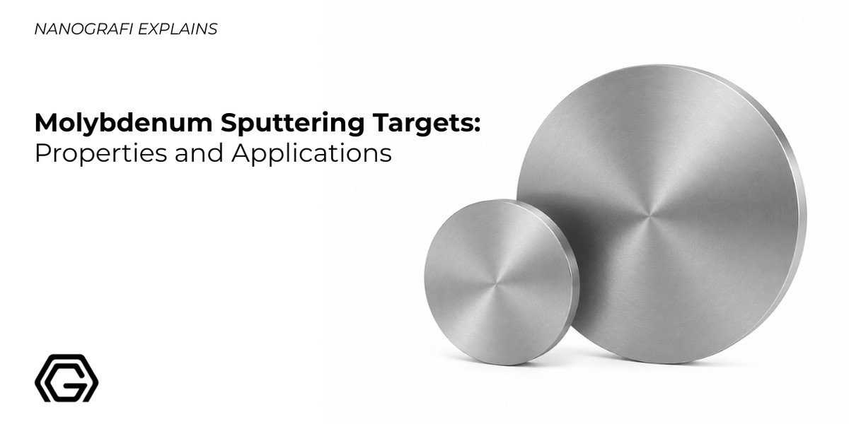
Molybdenum Sputtering Targets: Properties, Applications, and How to Choose the Right One
Molybdenum (Mo) sputtering targets are among the most widely used refractory-metal targets in physical vapor deposition (PVD), valued for the combination of a very high melting point, low electrical resistivity, and strong resistance to electromigration. These properties make molybdenum thin films a standard choice for gate electrodes, source/drain contacts, and back-electrode layers across the display, semiconductor, and thin-film photovoltaic industries. Because so many industries rely on the same basic material for very different jobs, it is worth understanding exactly how the process and the target itself work before choosing a grade, since the "right" molybdenum target for a solar cell manufacturer can be the wrong choice for a semiconductor fab.
What Is Sputtering?
Sputtering is a PVD technique in which a solid target is bombarded with high-energy ions, typically generated in a plasma by a DC or RF magnetron source, causing atoms to be ejected from the target surface and deposited as a thin, uniform film on a substrate such as glass, silicon, or a polymer web. The energetic ions transfer momentum to the atoms at the target surface, triggering a small collision cascade; when enough energy reaches an atom near the surface, it is ejected and travels toward the substrate, where it condenses into a continuous film. The underlying physics of the sputtering process has been studied since it was first observed as a natural phenomenon in gas-discharge tubes, and modern production lines now rely on several distinct sputtering process types, from simple DC diode systems to magnetron and reactive sputtering, each suited to a different combination of target material and film requirement.
Because sputtering allows tight control over film density, stress, and microstructure by adjusting parameters such as chamber pressure, target-to-substrate distance, and applied power, it remains the preferred technique even as newer deposition methods, such as atomic layer deposition, have matured for very thin or highly conformal films.
Why Molybdenum?
Pure molybdenum has a melting point of roughly 2,623 degrees Celsius and an electrical resistivity of about 5.2 microohm-centimeters at room temperature, giving it excellent thermal stability and conductivity for DC magnetron sputtering. Combined with a low coefficient of thermal expansion and good resistance to electromigration, this makes molybdenum films attractive wherever a conductive or barrier layer has to survive repeated thermal cycling without degrading. Molybdenum also bonds well to a range of substrates and can be alloyed with elements such as niobium or tantalum to fine-tune resistivity and long-term film stability; alloyed Mo-Nb or Mo-Ta targets typically show somewhat higher resistivity than pure molybdenum but reduce drift in film properties over time, which can matter more than raw conductivity in some production environments.
Typical applications include:
- Gate electrodes and source/drain metallization in TFT-LCD and OLED backplanes
- Back-contact and Mo/MoSe2 interface layers in CIGS thin-film solar cells
- Barrier and adhesion layers in semiconductor interconnects
- Decorative and functional coatings on glass and metal substrates
- Metal gate electrodes and tunable-work-function layers in advanced CMOS devices
Molybdenum is not the only material doing similar work in a sputtering chamber. Platinum sputtering targets are chosen for their oxidation resistance in harsher environments, tungsten disulfide targets offer a lubricating film with a very different friction profile, and titanium, lead, and zirconium targets round out the set of metals most commonly compared against molybdenum for barrier and electrode layers.
How Molybdenum Sputtering Targets Are Manufactured
Most molybdenum sputtering targets start as molybdenite ore, which is concentrated by flotation and then converted to molybdenum oxide through roasting. The oxide is reduced to pure molybdenum metal by hydrogen reduction, then processed into fine powder through atomization or mechanical milling. This powder is pressed and sintered at high temperature and pressure into a dense billet, which is then machined into the final target shape and, for larger diameters, diffusion-bonded to a copper or aluminum backing plate for improved heat dissipation during sputtering.
Quality control at each stage typically includes checks for purity, density, grain size, and the absence of internal defects, using techniques such as X-ray diffraction, scanning electron microscopy, and energy-dispersive X-ray spectroscopy. Manufacturers increasingly report relative densities above 99.6% for premium-grade targets, since higher density directly reduces the risk of arcing and particle generation during long production runs.
Molybdenum vs. Molybdenum Compound Sputtering Targets
Buyers frequently need to choose between elemental Mo and its compounds, so here is a quick comparison:
| Target | Main use case | Key property |
|---|---|---|
| Mo (pure metal) | Gate electrodes, TFT-LCD, CIGS back contact | High conductivity, high melting point |
| MoS2 | Dry-lubricant coatings, 2D semiconductor films, flexible displays | Low friction, tunable band gap (about 1.8 eV) |
| MoSi2 | High-temperature protective and resistive coatings | High melting point (about 2,050 degrees Celsius), oxidation resistance |
MoS2 belongs to the transition metal dichalcogenide family and forms a layered hexagonal structure, with molybdenum atoms sandwiched between planes of sulfur atoms, a structure explored in more depth in our article on Molybdenum Disulfide (MoS2) properties and applications and its growing role in automotive coatings and components. This layered arrangement is what gives MoS2 both its low-friction, solid-lubricant behavior and its usefulness as a two-dimensional semiconductor for flexible displays and transistors, a very different role from the purely conductive one that pure molybdenum plays. Where an application calls for an oxide precursor instead of a metallic or sulfide target, molybdenum oxide nanoparticles are typically the better starting material.
How to Choose Purity, Size, and Thickness
- Purity: 99.95% is the standard grade for most display and solar applications; higher purities (99.99% and above) reduce particle generation and are preferred for advanced semiconductor nodes. Nanografi's molybdenum sputtering targets, MoS2 sputtering targets, and MoSi2 sputtering targets are all supplied at these standard purity grades, with the wider sputtering targets catalog covering other elements and compounds for comparison.
- Grain size and density: A fine, uniform grain structure, with a relative density above roughly 99.6%, minimizes arcing and particle defects during long sputtering runs.
- Size and thickness: Common target diameters range from 1 inch to 8 inches, with thicknesses of 0.125 inch and 0.250 inch being the most requested for planar magnetron systems. Match these dimensions to your chamber and magnetron configuration before ordering, since an incorrect fit can shorten target life or cause uneven erosion.
- Bonding: Larger targets are often diffusion-bonded to a copper backing plate for better heat dissipation, while smaller targets can be used unbonded in many systems.
- Target shape: Planar targets remain the most common format for R&D and small-batch production, while rotatable targets are increasingly used in high-volume glass-coating lines because they offer more efficient material utilization over the target's lifetime.
When the process calls for a powder feedstock rather than a solid target, such as for thermal spray or additive manufacturing, molybdenum micron powder and molybdenum nanoparticles fill that role instead.
Handling and Storage Considerations
Molybdenum targets are generally stable at room temperature and do not require special atmospheric storage, but they should be kept dry and free of surface contamination, since oxide layers or moisture on the target surface can cause inconsistent sputtering rates or arcing during the first minutes of a run. Many operators run a short pre-sputter or "burn-in" step with the shutter closed before starting deposition, which cleans the target surface and stabilizes the plasma before the substrate is exposed.
Frequently Asked Questions
What purity do molybdenum sputtering targets usually come in? Most commercial targets are supplied at 99.95% or 99.99% purity, with higher grades available for advanced semiconductor applications.
What thickness should I choose? 0.125 inch and 0.250 inch are the most common thicknesses; the correct choice depends on your target holder and the erosion life you expect from the target.
Can molybdenum targets be bonded to a backing plate? Yes. Bonded targets are common for larger diameters (6 to 8 inches) to improve thermal management and reduce cracking risk during sputtering.
How long does a molybdenum sputtering target last? Target life depends on thickness, power density, and erosion pattern, but most planar targets are used until roughly 30 to 50 percent of the material has been eroded, after which redeposition and particle generation increase.
Do molybdenum targets need to be pre-sputtered before use? A short pre-sputter step is generally recommended to remove any surface oxide or contamination and to stabilize the plasma before coating the actual substrate.
References
Li, X., & Zhu, H. (2015). Two-dimensional MoS2: Properties, preparation, and applications. ScienceDirect.
Plansee SE. (n.d.). Molybdenum sputtering targets. Retrieved 2026, from https://www.plansee.com/en/products/molybdenum-sputtering-targets.html
PatSnap Eureka Materials. (2026). Molybdenum sputtering target: Advanced manufacturing, microstructural engineering, and performance optimization for semiconductor applications. https://eureka.patsnap.com/materials/mo-sputtering-target-semi
Sobayel, K., Akhtaruzzaman, M., Rahman, K. S., Ferdaous, M. T., Al-Mutairi, Z. A., Alharbi, H. F., Alharthi, N. H., Karim, M. R., Hasmady, S., & Amin, N. (2020). WS2: A new window layer material for solar cell application. RSC Advances.
Sputtertargets.net. (2026). Everything you need to know about molybdenum sputter targets. https://www.sputtertargets.net/blog/everything-you-need-to-know-about-molybdenum-sputter-targets.html
Vreeswijk, M. J. G., Verlaan, V., Houweling, Z. S., Cabo, M. F., van Deelen, J., Poodt, P., Schropp, R. E. I., & van Erven, A. J. M. (2007). Deposition of high-quality Mo thin films by magnetron sputtering. Applied Surface Science, 253(14), 6338-6342.


Recent Posts
-
Handling and Storage Best Practices for Metal Oxide Nanopowders
A metal oxide nanopowder is bought for a property that a coarse powder cannot deliver: a specific su …1st Sep 2026 -
Activated Carbon vs Zeolites vs MOFs: Which Adsorbent Material Should You Choose?
Activated carbon, zeolites and metal-organic frameworks (MOFs) represent three distinct adsorbent cl …20th Aug 2026 -

Anti-Icing Nanocoatings: How Nanomaterials Prevent Ice Formation on Aircraft, Wind Turbines, and Power Lines
Ice accretion is not a cosmetic problem for industrial equipment operating in cold climates. On airc …12th Aug 2026